Sampling circuit
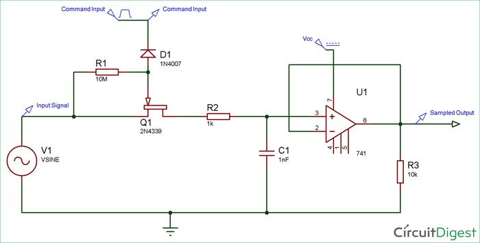
The sampling circuit has an analog signal input, a control signal input and an analog signal output. The function of this circuit is to receive the input voltage at a certain time and keep the voltage at the output until the next sampling starts. The sampling circuit usually consists of an analog switch, a holding capacitor and a non-inverting circuit with a unity gain of 1. Sampling works in one of two states, sampling state and holding state. In the sampling state, the switch is turned on, and it tracks the level change of the analog input signal as quickly as possible until the hold signal arrives; in the hold state, the switch is turned off, the tracking process stops, and it stays before the switch is turned off. The instantaneous value of the input signal.
Principle
Agilent’s latest 90000X series oscilloscope uses indium phosphide (InP) semiconductor materials to design the front-end chip of the oscilloscope, making the hardware bandwidth break through the 16GHz bottleneck, reaching the order of 32GHz, and breaking the future The bottleneck of oscilloscope bandwidth development.
However, I think the most important breakthrough is the sampling circuit technology. The design of the new sampling circuit has increased the accuracy between samples from 1ps to 50fs, while overcoming the limitations of ADC bandwidth and the development of future sampling rates. Bottleneck. This is the key point.

The front-end chip of 90000X oscilloscope, the chip integrates: 32GHz front-end amplifier, 22GHz trigger, 80GSa/s sample and hold circuit.
The sampling circuit design of 90000X is very worthy of our reference, especially in the case of domestic development of ADC encountered a relatively large bottleneck.
This sampling circuit separates the sample-and-hold circuit from the data conversion, and uses indium phosphide to design the sample-and-hold circuit (mainly composed of switches and storage/filtering) to overcome the bandwidth bottleneck. The accuracy of the sampling interval is determined by the delay line To guarantee (so it reaches the order of 50fs or lower), and the traditional ADC is used for data conversion (instantaneous DC signal data conversion) outside the front-end chip.
This achieves the purpose of high bandwidth, high precision and low cost.
The actual product performance measurement results prove that the design is very good, using 8bits ADC can reach more than 40dB spurious-free dynamic range.
What if a 12bits ADC is used? The result will exceed our imagination.
Therefore, this technology can be used for reference in China, using the indium phosphide that has been studied for sampling/switching/holding/filtering circuit, and the use of low-speed traditional ADC for data conversion, so that it can achieve: high bandwidth, high Sampling rate, high-precision analog-to-digital conversion products with high digits.
